展示全部
Scontel高效率QE>90%超导纳米线单光子探测器
1ps超高分辨率时间相关单光子计数器(TCSPC)
荧光寿命成像FLIM入门套件
中红外(MIR)超导单光子探测器
单光子探测器阵列SPAD23
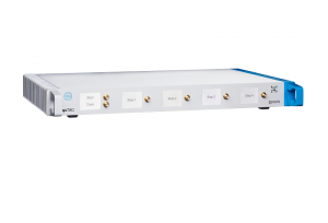
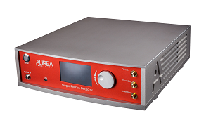
900~1700nm单光子探测与计数一体机
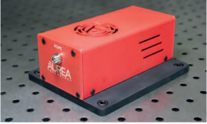
900 —1700nm近红外单光子探测器
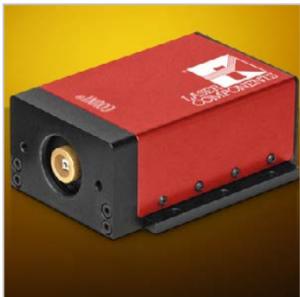
NIR单光子探测器模块
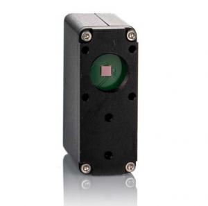
可见光-近红外单光子探测器
SiPM单光子探测器
370-900nm超低暗计数单光子探测器
Scontel超导纳米线单光子探测器(需要制冷腔)
SPADλ线阵单光子相机
一.介绍SPD_NIR为900nm至1700 nm的近红外范围内的单光子检测带来了重大突破。 SPD_NIR建立在冷却的InGaAs / InP盖革模式单光子雪崩光电二极管技术上,是NIR单光子检测器的第一代产品,可同时执行同步“门控”(GM)和异步“自由运行”(FR )检测模式。 用户通过提供的软件界面选择检测模式。冠jun级别的器件具有低至800 cps的超低噪声,高达30%的高校准量子效率,100 ns最小死区,100 MHz外部触发,150 ps的快速成帧分辨率和极低的脉冲 。 当需要光子耦合时,标准等级可提供非常有价值且经济高效的解决方案。基于工业设计,该设备齐全的探测器不需要任何额 ...
单光子探测器暗计数在激光远距测距的重要性激光测距技术在民用、军事等方面均有广泛应用,远距离测距的需求也日益增加。下图中给出了超导纳米线单光子探测器应用于激光测距的基本原理图。激光器为1064 nm,回波经透镜、光纤耦合至单光子探测器,光路可调节耦合过程中存在的损耗。激光发射同时触发计时,单光子探测器响应回波光子以及噪声光子,结束计时,此周期为1ms。单脉冲回波光子数n0。可由式得到:为激光功率峰值,Δt为激光脉冲宽度,D为接收孔径,分别为反射/接收光学效率,p为目标物反射率。下图为单光子探测器不同条件下的暗计数对信噪比(SNR)的影响,横轴为脉冲积累次数, 纵轴为信噪比,可知,回波率较高时(近 ...
前,可用的单光子探测器件有:光电倍增管(PMT),工作在盖革模式下的雪崩光电二级管(APD)等。在400至900nm光波段,以硅APD为敏感元件的单光子探测器性能良好,暗计数小于25cps,量子效率在650nm附近可高达到70%。但由于带隙宽度的限制,硅APD对波长1微米以上的光没有响应。在近红外光波段(1100~1650nm),目前性能很好的是基于铟镓砷()APD的单光子探测器,其量子效率在1.55μm波长处能达约25%,暗计数约10^3cps左右。总体而言,不论光电倍增管还是基于APD的单光子探测器,其量子效率、暗计数等性能远不能满足量子信息计数发展的需要,特别是针对所谓的线性量子计算,对 ...
、(超导)单光子探测器可以搭建一套基于时间相关的非视域探测系统,实现对视域外物体的高精度的定位,并初步得到物体的表面轮廓。实验过程:超快脉冲激光器发射出脉冲激光,经扫描振镜反射后照射在中介墙面上,经墙面漫反射后部分散射到达拐角处的物体,再经过物体表面反射后极小部分携带着物体信息的光返回墙面被单光子探测器(SPAD)所接收。脉冲激光器的电同步信号与探测器探测到的光子产生的脉冲序列,分别接入TCSPC模块的“开始”与“结束”通道,得到光子—时间的时间直方图,基于时间直方图的信息,通过椭球层析算法即可重构出拐角处物体的信息。图4.2.1实验装置图上述实验图为山东大学孙宝清教授组的实验场景及成像结果图 ...
超导纳米线单光子探测器简介:展示了一种在1550 nm处具有高效率、低于0.1 Hz的暗计数率和低于15 ps的timing jitter的自由空间耦合超导纳米线单光子探测器。作者:Andrew S. Mueller, ...Matthew D. Shaw链接:https://doi.org/10.1364/OPTICA.444108LETTERS1.标题:使用时间延迟积分连续流式压缩高速摄影简介:开发了连续流式压缩高速摄影,它可以以前所未有的空间带宽时间积记录动态场景。通过以时间延迟积分方式执行压缩成像,实现以200 kHz的频率连续记录了0.85兆像素的视频,对应于每秒170吉像素的信息通 ...
,由于大多数光子探测器是二维(图像传感器)、一维(线传感器)或零维(单像素传感器)的,用低维传感器采集高维全光函数通常需要沿另一个维度进行大量扫描。例如,为了获取全光数据立方体,高光谱成像仪通常在空间域或光谱域中进行扫描,从而导致采集时间延长。相比之下,像映射光谱仪(image mapping spectrometer, IMS)、编码孔径快照光谱成像(coded aperture snapshot spectral imaging)和计算机层析成像光谱(computed tomography imaging spectrometry)等快照技术将三维全光数据立方体以光学手段重新映射到二维探测 ...
所示。来自单光子探测器的光电子信号脉冲和来自激光器的参考脉冲输入到延迟链中。时序逻辑查看延迟链中的数据,识别单光子和及激光脉冲的开始-停止对,并以此方式确定单光子在激光脉冲序列中的时间位置。然后,可以根据这些数据,建立通常的TCSPC/FLIM光子分布。TCSPC技术所基于的原理是:在记录低强度、高重复频率的脉冲信号时,由于光强很低,以至于在一个信号周期内探测到一个光子的概率远远小于1。因此,没有必要考虑在一个信号周期内探测到几个光子的情形。只要记录这些光子,测量它们在信号周期内的时间,并建立光子时间分布的直方图就足够了。TCSPC技术的基本原理如图所示。探测器的输出信号是对应于探测到单个光子 ...
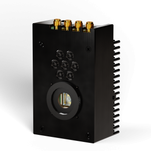
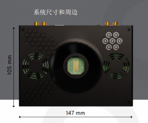
辨率图像。单光子探测器阵列SPAD23技术源于代尔夫特理工大学和洛桑联邦理工学院 7 年的研究工作和 6 项独特技术。它是由23个六角形封装的单光子雪崩二极管组成的探测器阵列(SPADs),具有更高的灵敏度和更低的噪声。这款单光子探测器阵列SPAD23在其宽探测谱段内拥有>50%的探测效率,<100cps的暗计数水平,且因其独特的半导体工艺及设计实现了前所未有的填充因子>80%。这款带有时间标记功能(Time Tagging)的SPAD23整体尺寸只有信用卡大小,是荧光显微和量子信息领域的理想探测工具。https://www.auniontech.com/details-1676. ...
用SPAD512S在3D成像中的应用在从空间成像到生物医学显微镜、安全、工业检查和文化遗产等众多领域,对快速、高分辨率和低噪声3D成像的要求非常高。在这种情况下,传统的全光成像代表了3D成像领域最有前景的技术之一,因为其超高的时间分辨率:3D成像是在30M像素分辨率下每秒7帧的单次拍摄中实现的,对于1M像素分辨率为每秒180帧;无多个传感器,近场需要耗时的扫描或干涉技术。然而常规全光成像导致分辨率损失,这通常是不可接受的。我们打破这种限制的策略包括将一个全新的和基础性的采用上一代硬件和软件解决方案。基本思想是通过使用新型传感器来利用存储在光的相关性中的信息实现一项非常雄心勃勃的任务的测量协议: ...
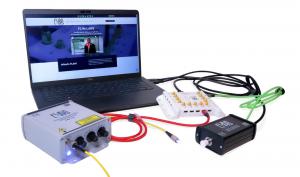
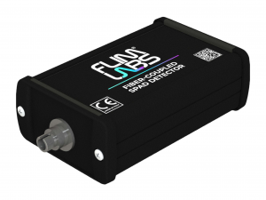
、SPAD单光子探测器与荧光寿命成像FLIM软件,并在您需要时提供恒比鉴相器模块。图4 FLIM LABS的荧光寿命成像FLIM入门套件FLIM数据采集卡TDC:我们的紧凑型USB 供电数据采集卡专为荧光寿命成像和光谱测量而设计。其基于FPGA的可定制技术,尺寸101x139x28mm,重量轻(仅120克),总计26个I/O通道可分辨荧光寿命50ps,死区时间1.5 ns,计时精度(σ/√2)300ps,24 或 48 ps 时间 bin 分辨率,并能通过USB3.0与PC软件直接连接,无需额外供电。光纤耦合皮秒脉冲激光器模块:我们的激光器模块可用波长有405、445、488、520、635 ...
或 投递简历至: hr@auniontech.com